Blog
nVidia Optimus and ASUS UL50VF: An Invisible Game Changer
Writing a review is a tought process and often we, reviewers found ourselves in between a rock and a hard place and finding a place to write in peace is sometimes a great challenge. Given the subject of this story, I decided to write an article 12 kilometers above the ground, between San Francisco and Frankfurt. The original itinerary was supposed to bring me through Washington DC back to Europe, but due to the snow that shut down airports on East Coast, I took the San Diego – San Francisco – Frankfurt route.
The only thing not written in the air will be the performance results. Both Anshel and I worked extensively with the test unit over the course of two weeks as we tried to find as many bugs as possible, to see if this technology is really ready or not. Prior to boarding, we received new drivers from nVidia, as the ones we originally had on the notebook had some issues we’ll elaborate on a bit later. This required us to re-test all of the benchmarks and well, miss the launch on Tuesday. We hope it was worth the wait.
Challenges of notebook design today
In order to understand why nVidia went through all the grief of creating the Optimus Technology, it is necessary to get down to the essentials of notebook design. Notebook design is tough, there isn’t any question about it. Packing everything in a small compact format, often smaller than a full-sized PC keyboard with a screen that folds on top carries a lot of complexities and it is very easy to make a cardinal design error which could cost a lot of money and market share.

Matt Wuebbling, Senior Product Manager for Notebook at nVidia details the situation on market today
As notebooks growing in popularity and their market share increases, expectations from the consumers are growing day by day, not caring about the actual physical implementation. Naturally, this leads to the market wanting gaming performance and wanting discrete graphics. The problem with discrete graphics is that GPU will consume power regardless of being bogged down to a level of display image only, or when the GPU is cranking at full speed. Both AMD and nVidia made great improvements with their internal power designs, however – even when those designs reached Intel’s level of efficiency, OEM vendors are still forced to buy Intel’s integrated graphics, as was a part of the Centrino platform, and is an integral part of the chipset. Disabled or not, that part will also consume power. Enter the world of Hybrid Graphics.
Launched with Sony VAIO SZ-110B in April 2006, Hybrid Graphics originally required a reboot – as you can imagine, not exactly a seamless experience and if you’re doing this while running on a battery – the user would lose additional battery life during the boot up process. The second generation was introduced in 2008 with nVidia-powered notebooks such as the ASUS UL50VT or AMD-powered notebooks such as HP Envy 13. Matt Wuebbling, Senior Product Manager for Notebook graphics demonstrated us how the switching of graphics worked until this date and long story short – it sucks. The second generation ditched the reboot requirement, but we still had a blank screen, if you had an application that ran a DirectX window, it would not switch regardless of the content etc.
The reason for all the issues was the way how companies implemented discrete graphics. Unfortunately, it isn’t as simple as we imagined. One of the main culprits of combining integrated and discrete graphics is the necessity to use a MUX Switch for each and every connection you have on the motherboard. As you can see on the images, a MUX Switch isn’t exactly easy to implement into the design.

Upcoming Arrandale [Core i5] motherboard that utilizes GeForce G210M and has a bunch of MUX switches

How a MUX Switch Works – about all that additional wiring added to an already complex design
A hardware switch wasn’t the only thing a company needed to do in order to enable Hybrid Graphics – nVidia also had to bundle Intel’s driver inside its own to make it work.
At the end of the day, nobody was happy. The notebooks cost much more than they should have, additional time would be lost in qualification, and users didn’t get the experience they wanted. We now Enter the world of Optimus.
nVidia Optimus Technology

The main idea that guided the teams lead by Sasha Ostojic, Director GPU Software and Sridhar Pursai, Director Platform Engineering
When we first learned of the nVidia Optimus Technology back in November, it looked quite promising – even though we had no idea how nVidia would offer seamless switching. I admit I was wrong, but my idea was something in the lines of new NVIO chip that is usually bundled with high-end GPUs and that the new NVIO chip would accept signals from Intel or AMD integrated graphics part. This time around, I am really glad I was wrong. We received an invite to an Optimus Deep Dive event featuring us and 13 other journalists across the globe. The Optimus Deep Dive event took the better part of one cold Monday in January.

nVidia Optimus Technology – Good bye MUX, Software overlay controls the both GPUs
To answer immediately, Optimus is nothing else but a combination of software and internal hardware controlled graphics switching. Forget about expensive MUXes, this is an intelligent way of taking over the processing of DirectX/OpenGL calls the moment they’re made. Optimus works by leaving the Intel’s Display Driver to display image on the screen and actively monitoring everything that is happening in relation to displaying image. The library of applications inside nVidia’s driver will automatically react and switch to the GPU as soon as it detects application profile where nVidia’s GPU would do much better than integrated graphics.
The interesting bit about this detection is that nVidia will offer automatic profile updating – when an Optimus-powered notebook asks for updates, it should download new application profiles too, as well as some fixes. This is not an automated driver update – Optimus v1.0 will offer profile updates only, and the company said it is looking into the future variants of Optimus to bring as much seamlessness as possible. Naturally, in order to enable automatic driver component update, nVidia would have to change its internal driver stack. This is also the reason why ATI fell flat on their promise to offer automatic driver updates with Catalyst drivers [back in 2003].

Optimus Copy Engine is the secret to how Intel’s IGP sees the finished frames rendered by nVidia GPU
The second part of the Optimus technology is actually a hardware one, but not the NVIO or anything similar. Rather, nVidia’s Optimus-capable GPUs feature “Optimus Copy Engine”, a parallel pipeline next to the 3D Engine one. What Copy Engine does is takes the finalized rendered engine created by the 3D Engine and copies the contents from on-board memory to the system memory – which is then taken by Intel’s IGP and displayed on frame-by-frame basis. This approach removed a lot of unnecessary overhead and more importantly, killed latencies that would happen if the company didn’t put the afore mentioned Optimus Copy Engine.
Starting with GeForce G200 series, all nVidia GPUs have built-in support for Optimus technology. According to nVidia, even the upcoming GF100 architecture will support Optimus not just in notebook variants, but in desktop as well, on a top-to-bottom basis. The company is planning to stop Intel’s rising share in graphics by offering a complementary add-on, rather than a complicated discrete add-on to the design.

Launch Platforms
Naturally, in order to adopt the technology, you need a lot of partners behind your back. Starting with this week, ASUS launched five notebook designs on world-wide basis, while EU-oriented Medion launched a notebook for European markets. Six publicly announced designs does not seem like a great deal, but that is a natural consequence of launching the technology prior to China and Taiwan shutting down. As of today [Friday, February 12, 2010], almost all of China and Taiwan shut down for Lunar New Year festival, with offices and foundries opening up in two weeks time, around February 22, 2010. After that, a mad rush to complete the designs to CeBIT will commence, and we should see at least 20-30 design wins on CeBIT 2010 in Hannover, Germany [March 2-6]. For Back To School 2010, nVidia expects to ship around 50 design wins, including Acer, Dell, HP and the rest of top tier vendors.
The Apple Connection
The relationship between Apple and nVidia has always been an interesting one. After all, Apple came on board and committed to OpenCL after nVidia sent engineers with a working demo of the OpenCL platform back in May 2007. A few months after, Apple launched second generation MacBook Pro and iMacs featuring nVidia GeForce 8-series GPUs and later, GeForce-9 series chipsets – much to the surprise of the analyst and media communities. According to our sources, that demo was the reason why nVidia ended up in Mac machines, as Steve himself was a true believer in the technology demonstrated to him.
After learning that, it was quite funny hearing “Apple is the driving force behind OpenCL” mantra and how some vendors criticized nVidia for forcing proprietary standards while at the same time, we might even say that OpenCL would not have happened if there wasn’t for the company exactly criticized for the lack of “openness”. But that’s just how this game goes.
When Intel announced they’re integrating their graphics subsystem with their 32nm products, our sources at Apple were adamant they will not go with the Arrandale-based notebook unless a better graphics switching solution was found. I was personally told “Steve doesn’t trust them [Intel]. We got burned with mediocre graphics on Apple TV and MacBooks and that will never happen again.” To make the matters worse for Intel, there seems to be a lot of tension between Apple and Intel as far as patents go. It isn’t widely known, but Intel patents a lot of non-core business related patents, with one of them being keyboard air intake. Apple used this technology on a lot of their products and when Taiwanese vendors started to utilize the same technology, the giant from Cupertino started to pressure Intel not to allow this to happen and got owned in the process.
Getting back to the subject, on the subject of whether or not we are going to see an Apple refresh using Arrandale thanks to the Optimus technology, your guess is as good as mine. If it does happen, remember where you read it first. For now, Apple’s official stance is that Arrandale, just as any other part with Intel integrated graphics, will rot in hell. Who is to blame for that, given that Intel’s integrated graphics can normally run Windows Vista and Windows 7 Aero interfaces, as well as Project Looking Glass and its “offspring” Compiz on Linux. Thus, we believe nVidia Optimus technology has a really good chance of winning the Apple deal all over again.
ASUS UL50VF Laptop
In order to demonstrate the functionality of the Optimus technology, nVidia provided us with an ASUS UL50VF notebook. This is an Optimus version of their UL50VT notebook – The UL50V Series comes with a somewhat large 15.6” chassis, and an Intel Core 2 Duo U7300, which is a dual-core CULV processor ticking at 1.30 GHz using Front Side Bus at 200MHz QDR [800MHz]. This is not the final clock, as there is enough cooling overhead for overclocking mode called Turbo33. As the name states, power consumption will almost triple to around 25-30W as the CPU will start operating at 1.73 GHz using the 266MHz QDR [1066MHz] Front Side Bus.
The GPU in question is a GeForce G210M, built using the 55nm process technology at TSMC. This low-cost, DirectX 10.1 supporting GPU packs only 16 cores that work at 1.47GHz, while the reminder of the GPU ticks at 606MHz. Memory controller is merely a 64-bit one, connecting with 512MB GDDR3 memory ticking at 790MHz in DDR mode [1.58 GHz data rate], resulting in a video memory bandwidth of a mere 12.64GB/s. Given that the current top single-GPU desktop card from nVidia delivers 159GB/s [default clock, not counting factory overclocked cards], while the top single-ASIC model from AMD pitches in 153.6GB/s, you can see that this board has 12.57 times LESS the memory bandwidth, 15 times less shader cores [they’re even not the same architecture]… overall on paper, this GPU looks like complete excuse for nVidia’s coined-term “Graphics Processing Unit”. Graphics Displaying Unit was more like it, we thought in our heads.
The graphics part is connected to a 15.6” LCD display using a 16:9 resolution of 1366×768 pixels. The screen will fit the whole 720p video with no issues [no black horizontal lines] and this is the optimal resolution as far as the 16-core GPU is able to handle. Given the price of $799, don’t be surprised to hear that the screen isn’t of best quality – ASUS used a TN panel which are usual at this price level. The company did implement an LED backlight which compensates for the TN panel. If you look at the screen, you’ll be hard pressed to know the difference between IPS, MVA, PVA or a TN – the only giveaway is that white is a bit warmer than on IPS/MVA and the viewing angles.
The notebook also comes with 4GB of DDR3-1066 memory and a Seagate Momentus 5400.6 320GB hard drive.The system is rounded off with a Matshita UJ982AS, SATA DVD-RW drive.
As it usually goes, connectivity is perhaps the most important part of any notebook and chosing the wrong wireless or Bluetooth chip can significantly limit the range and also, reduce the life of the battery. Luckily, ASUS went with the Atheros AR8131 Gigabit Ethernet and AR9285 Wireless controllers and Atheros is a known figure in the world of power saving wireless chips. Just compare the battery life between the iPhone and Blackberry Bold if they both run 3G. According to one of our sources, Atheros saves 3-5% of power when compared to Marvell and Intel Gigabit Ethernet, and around 7% of power when comparing Intel vs. Atheros Wireless components.
In order to power all these components, Asus installed an 8-Cell, 5600 mAh, or 84 Wh battery. This is the highest capacity the company has in store, and according to the manufacturer, it should be good for “up to 12 hours of battery life”. Given that we’re writing this piece in the middle of crossing the Hudson Bay in Canada, five hours into the flight.
Exterior

ASUS UL50VF in all of its beauty. Photo: Goran Legovic
ASUS UL50VF is a product that shows the company’s strengths and weaknesses at the same time. When you take a look at it, first thing you’ll notice is the aluminum cover with an ASUS logo and it definitely looks more than you paid for it. The notebook is really slim – something you don’t expect from a 15.6” case.
The left side features a power connector, heat exhaust, multi-card reader, HDMI, two USB ports and audio connectors. The right side only features an analog D-SUB [when will these analog projectors finally die out?], 1GbE port, Optical drive and a single USB port. Speakers are located at the front side, just below the ridge. When you open the UL50VF, you’ll be greeted with a lot of shiny black plastic which looks just like the price you paid for it.
We really like the fact that there were only two stickers on the notebook, and they aligned nicely with the notebook. Yes, we do understand that a final retail version has to come with a Windows 7 sticker, but if I were you, I would remove every sticker sans one or maybe two nVidia ones.

Everything is stylish and there aren’t any excessive design faults typical for Far Eastern vendors
The full-sized keyboard is a delight to type on. It is really good to see that more and more notebooks are adopting Intel’s genius patent of taking the air from the holes in the keyboard for cooling as it not just cools down the components but also creates a tiny amount of airflow around the keyboard. No sweaty palms here, that is. There are only three special keys on the whole laptop: The ExpressGate button is located above the Escape key, Power button is located on the right, above the End key, and large single key in the middle for left- and right-click below the touchpad. Every other command is located on some of the keyboard keys and you have t ouse a Function Key plus that particular key to execute command [WiFi On/off, Standby Change Screen, Play/Pause, loudness etc.].
The second thing that we really liked is the inclusion of a multi-touch touchpad. Asus was the first company to incorporate multi-touch pads even on their netbooks, back in the day when Apple was only switching to the PC platform.
The weakest part of this whole notebook is an optical drive unit. It’s not an issue of quality as it is rather an issue with the design. The optical unit is located on the right side of the notebook and there would be nothing wrong with that if there wasn’t for the eject button. You’ve guessed it right; eject button is located exactly at the ridge and well, you will accidentally open it… and again, and again and again. In the first week of testing, the unit opened at least a dozen of times. Given that the world is moving away from the optical drives, we hope that future versions will have a bracket in the box, so that you can put the optical drive out and who knows, gain maybe 5-10 minutes to battery life.
Experience
Our testing actually begun – with a bug found in the first few minutes of working with the notebook, which was resolved after talking to nVidia and ASUS. The bug was something atypical – if you would click on full-screen when playing a Flash video, the screen would turn black. That’s right, no YouTube or just about any other Flash-based video file. The culprit here was a 1080P trailer for Avatar [seen the movie four times in 3D]. As you might have guessed, this is not something you should experience… anywhere. Upon contacting nVidia, we were delivered a new driver. Following the installation of the 188.97 drivers and subsequent arrival in Zagreb on Sunday, we went on and re-did all the benchmarks using these drivers. According to Sean Pelletier, these are the drivers that users will experience when they purchase a notebook, so we went on and compared our previous benchmark runs to the newer one.
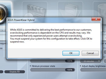
Our notebook booted at 1.3 GHz, but we wanted to see the 1.73 GHz as well, which can be easily activated by clicking on the battery icon in the taskbar, selecting the Power4Gear utility [on the left side of the Window] and setting the computer into a Turbo mode.
In order to overclock the CPU, the system will go down to standby, change the FSB speed from 200 to 266MHz and resume from standby. In a way, this reminded me of AMD-switchable graphics demo on HP’s Envy and the nVidia-switchable graphics on previous-gen ASUS CULV notebook, albeit much faster. Unfortunately for the whole Optimus experience, CPU clock change doesn’t go as invisible as the GPU on-off switch. While screen blinking and standby is a normal thing on non-Optimus UL50VT, UL50VF GPU switching works much better than the CPU one. It is exactly with this small thing – you start to see the real value of Optimus technology. No hassle, it just works. And when a friend asked me to summarize this technology in a plain language, I had only three words in mind: invisible game changer.

Power4Gear Hybrid application, where you can control all the power aspects of this notebook
The funny thing about this notebook is that it comes with a Chinese keyboard enabled by default. Thus, if you accidentaly press Ctrl+Space or Alt+Shift, the keyboard will change from English to Chinese – it might be a good idea to delete the Chinese keyboard layout as well. Unless you need it, naturally.
During our everyday work, we managed to get around 10 hours of battery life. Seeing 93% battery life stating “10hr00min remaining” brings something warm around the heart. Even though the specifications claim 12 hours, we were really happy with more than 10 hours of autonomy, which we used and abused during traveling. San Diego to Los Angeles and back, and the laptop had disabled sleep mode. The laptop also lived throughout the flight between San Francisco and Frankfurt, even though we did watch two movies – DVD version of YPF and a digital copy of our Star Trek Blu-ray [Thank You Dolby]. During playing both of the movies, G210 spun to life and took over, rather than 100% CPU utilization and choppy framerate on GMA 4500, as we experienced before. In my life, I’ve flown around 800,000 miles and during those countless hours up in the air [the movie is actually quite sad – I met very interesting people while taking a break from economy seating], I’ve used numerous notebooks from $500 to $6000 in value – from 12” SSD powered Samsung to 18.4” Toshiba Satellite Pro. Yet, incredible how it may sound, this $800 notebook is the most comfortable to fly with. Watching movies in HD without worrying should you start this or that one, but rather watching what you want – is priceless.
Performance – Real World
Loading Windows 7 System Properties reveals a score of 3.4, essentially a very poor result, especially when you see how that score was obtained: CPU scored 4.9, memory scored 5.4, Hard Disk scored 5.7… and the bottleneck was of course, Intel GMA 4500 – which scored only 3.4. The reason for G210M not activating lies in the way how Windows 7 runs the test – essentially, it didn’t allow the nVidia driver to activate the discrete GPU. This is something nVidia will probably work in the future but it isn’t exactly a show stopper.

Badaboom GPU transcoding – 38.6 frames per second sound and feel much better than 3-4 frames.
nVidia is heavily pushing video transcoding as a major thing – our sample came with Elemental Technologies Badaboom transcoding software. We also tried native Windows 7 transcoding, but given the limitations of native transcoder [transcoding is a drag and drop feature and you have to have a Windows Media Player compatible device – our BlackBerry Bold does not qualify], we went back to Badaboom faster than you could say windowsisaflesxibleoperatingsystemandallofthefeaturesworkasintended. The G210M is miles faster than a built-in CPU, as it can transcode the DVD to a Blackberry/iPhone resolution [480×240] at 39.1 to 40.1 frames a second. Overall, G210M left Core 2 Duo U7300 [3.1fps] in the dust, proving that for video transcoding, GPU is the right way to go.

APDFPR 5.03 Screenshot – GPGPU-accelerated password cracking on the go
There is an application that we really like is not as widely known to the general audience as the more visual Badaboom, but ElcomSoft provides GPGPU password recovery software. We checked the PDF password recovery software as sometimes, it can be a life saver. Yes, I personally know the story about trying to open a six year old PDF document with a different password than the ones you use today. The same thing applies to pretty much any password-protected file you might have created over the course of years and forgot about it. Going on a business trip and all of a sudden needing that Outlook .PST file you archived and forgot the password? Even with tiny 16 cores, ElcomSoft’s APDFPR 5.03 Enterprise Edition [Advanced PDF Password Recovery] shown impressive speed. At first, the application didn’t used the GPU, but after installing CUDA SDK on the system, we managed to get GPGPU rolling at an impressive pace. If we let the password cracker run on a CPU alone, it would take 170 days to crack the password. Running on GPU, it would take approximately two and a half days. ElcomSoft also creates password breakers for various file types and the company’s largest clients come from security, intelligence and counter-intelligence sector, which is usually always the first to jump the gun on the most advanced and powerful methods of getting the results done. As you’ve might have guessed, ElcomSoft adopted CUDA long time ago and is contemplating OpenCL when the standard matures.
Performance – Games
Now, the question that you all have is the same to the one I had. GeForce G210M and playing games? Essentially a four year old G80 architecture receiving its second silicon spin and, 16 puny cores, 512MB dedicated GDDR3 memory – how could that play any game? In other articles online, you probably saw results in 800×600, 1024×768 and so on. Here on Bright Side of News*, forget about running scripted benchmarks without looking at the screen. Our gaming resolution was 1366×768 and if this laptop could not pull it off, we would pretty much bury this notebook, as it would be completely deserved. Again, if you want to see 3DMarkVantage scores, look elsewhere – we took Futuremark’s Shattered Horizon for the ride instead.
We tested following titles:
- Batman: Arkham Asylum
- Day of Defeat: Source
- Left 4 Dead
- Left 4 Dead 2
- Need For Speed: SHIFT
- Shattered Horizon
- Star Trek Online
- Unreal Tournament 3
- World of Warcraft
We believe this combination of titles If you are wondering why we still use Unreal Tournament, the reason is quite simple – performance of UT3 on GeForce 8800GTX in screen’s native resolution is still our “1.0x” multiplier as far as performance goes.
We started our testing with Left 4 Dead 2 and were discouraged from the get go. According to Valve, our “optimal” configuration would be 800×600 resolution with some details set to high, some set to medium. There was not a snowball’s chance in hell I would play in that resolution; crank it up to 1366×768 pixel resolution, decreased image quality to medium and loaded the game. And imagine the surprise – the game ran well. The game runs on an average between 40 and 54 frames per second in every level we checked it, and it only choked by a second when your avatar is completely covered in ooze and getting hammered by numerous zombies. In Day of Defeat: Source, we played with all the settings either high or medium again, at 1366×768. Trust us, you don’t want to run a non-native resolution on any LCD screen.
Following this, we were encouraged and loaded up Need for Speed: Shift and again, with all the details set to low, the game flew as equally fluent as on my Quadro FX 4800 [desktop counterpart: GTX 260-192], albeit desktop version runs with all the details cranked up at 1920×1200. Gaming on the go slowly started to become a reality with G210M, a GPU which originally, I refused to review. Well, I guess Brian Burke is now eating those Griotte chocolates and drinking coffee, since my original reaction to G210M… well, let’s just say I didn’t had a nice opinion. Yet, this laptop actually works and it works with higher framerates than Acer Aspire 3D, which came with Mobility Radeon HD 4570. To make the matters worse for Aspire, that system came with 2.2 GHz Core 2 Duo with 6MB of L2 cache, 4GB of DDR3 memory.
Shattered Horizon proved a tough cookie for the system, given it only has a dual-core CPU and PhysX processing is using the GPU – we thought G210M was the issue, but the performance was equal in 1280×720 and 1366×768. Overall, you can expect 30-35 frames a second with occasional dips below – don’t turn around to Mother Earth, and well, we had issues playing the ISS level. But with details on low, it was pretty good. If you yearn for space action, Star Trek Online worked nicely both in space mode and on the ground. We predominately used medium details. Batman: Arkham Asylum worked at around 20 frames a second no matter what we did. Then again, if you wanted to play it on GMA 4500 – no way. On the other hand, World of Warcraft and Unreal Tournament 3 worked perfectly with details on the high side. We only needed to reduce the shadows and in case of WoW, leave Depth of View on stock levels, and 60 frames a second were there.
All in all, quite a compelling gaming experience – NFS, L4D2 and Star Trek Online all come with good framerates and if you’re into these type of games, you’ll enjoy.
Value
ASUS debuted the UL50 line of products with UL50VT for only $849.95 and drove the price down to $799.95 in most e-tail stores. The price for Optimus notebooks will remain the same – $799.95 i.e. ditching those MUX chips decreased the cost and there is no need for a price premium. Do bear in mind that upcoming Arrandale-based designs will reduce the price even more, since there is no mandatory Northbridge.
Getting back to UL50VF, take the following factors into equation: it is thin, it is light, has a discrete GPU and a battery good enough for transcontinental flight in Economy class. For less than a thousand dollars, you get a notebook that frankly, obliterates those notebooks with mediocre screen sizes and pretty much takes away a major reason of buying one: battery life.
We do have things on our wishlist that would warrant a price premium, but this is probably best valued notebook you can currently buy on the market and yes, no wonder that ASUS launched Optimus technology with this one.
Conclusion: nVidia Optimus Technology
In the end, there is no other choice but to give two awards. Firstly, the technology that made all this possible. nVidia Optimus Technology is an invisible game changer. You won’t see it in action unless you install the nVidia “I Am On, I am Off” utility, yet it works. This technology hits on many levels: with the lower bill of materials, driving down cost allows this elegant technology into the mainstream.
In a way, we feel that nVidia is going from being “just a hardware company” into a solutions company. That road is a very difficult one to take but the results are in – discrete GPU power is available today without the complexity of the MUX Switch design and user hinderance with those black screen flashes. Best of all – it comes with a good price. Given that upcoming mobile derivatives of GF100 design [we’re preparing a separate story on these GPUs] are all supporting this technology, the future is definitely bright. nVidia Optimus Technology fully deserves our Innovation award.

Conclusion: ASUS UL50VF
Looking at the spec sheet of this laptop alone, you could be forgiven for thinking it costs at least twice as much: brushed aluminum cover, fantastic keyboard that uses the same Intel-built design Apple adopted few generations ago, fantastic multi-touch touchpad, good 15.6″ LED-backlit screen and again, the most important bit – around 10 hours of battery life in a plane not by looking at Excel table alone, but watching movies as well. I thought long about this product and after my colleagues had a chance to try the machine, we came to the conclusion.
The UL50VF is a voice of new a rejuvenated ASUS that is now free of the power struggles that damaged the company in the past two years. The company can now push into higher gear and we would not be surprised if ASUS turns out to be the next company to overtake Dell and ultimately, HP and maybe even Acer.
ASUS’ UL50VF shows you what can be done in affordable package – a power saving CPU complemented with a good power saving GPU, delivered over 10 hours of battery life in real world, not using botched benchmarks. Given that we were able to watch HD movies 38,000 feet above the Atlantic and still land in Frankfurt with 20 minutes of battery left is a strong testament of just how balanced this design is. Playing Left 4 Dead 2 for five hours and not running out of battery was a dream, yet this product makes it a reality. For this balance alone we give ASUS UL50Vf our coveted Editor’s Choice award.

Original Author: Theo Valich
Webmaster’s note: This news article is part of our Archive, if you are looking for up-to date articles we would recommend a visit to our technology news section on the frontpage. Additionally, we take great pride in our Home Office section, as well as our VPN Reviews, so be sure to check them out as well.

PS5 vs. Xbox Series X: Which Gaming Console Is Right for You?

The Rise of International Basketball: Trends Reflected on Platforms Like Bizbet

The Mobile Testing Lifecycle: From Planning to Execution

Alcohol and Women: Navigating Unique Risks, Health Impacts, and Effective Treatment Strategies

How to Develop a Data-Driven Crypto Trading Strategy in 2026

Cloud Dancer Is the White Everyone Wants at Home This Winter: Here’s What Makes It So Popular

How Premium Corporate Gifts Became a Driver of Customer Acquisition in Financial Services

Top 4 Project Management Tools to Use for Your Business

Best Chemical Testing Lab in Malaysia – Biochem Laboratories
